Silicon Carbide silicon carbide nozzle in Optoelectronic Devices
Silicon Carbide (SiC) has emerged as a promising material for optoelectronic devices due to its unique combination of superior physical and electronic properties. This article explores the various aspects of SiC in the realm of optoelectronics, delving into its structure, properties, applications, and future prospects.
Structure and Properties of Silicon Carbide
Crystal Structure
Silicon Carbide belongs to the family of wide bandgap semiconductors, characterized by its hexagonal crystal structure. It exhibits polytypism, with common polytypes including 3C-SiC (cubic), 4H-SiC, and 6H-SiC (hexagonal). The crystal structure significantly influences its electronic properties and suitability for optoelectronic applications.

Electronic Properties

SiC has a wide bandgap ranging from 2.3 eV for 3C-SiC to 3.3 eV for 6H-SiC, depending on the polytype and doping levels. This wide bandgap allows SiC-based devices to operate at higher temperatures and voltages, with reduced leakage currents compared to silicon-based counterparts. Additionally, SiC exhibits high electron mobility, thermal conductivity, and resistance to radiation damage, making it ideal for high-power and high-frequency applications.
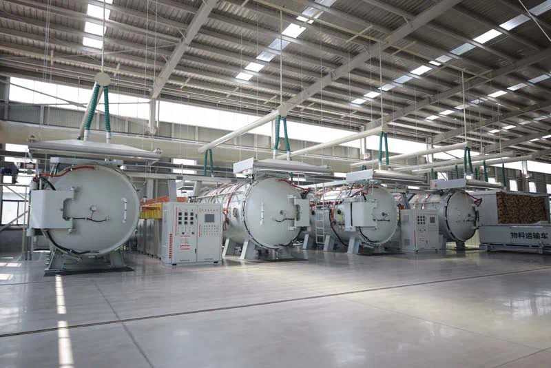
Fabrication Techniques for SiC Optoelectronic Devices
Growth Methods
The fabrication of SiC optoelectronic devices involves several key growth techniques:
Chemical Vapor Deposition (CVD)
CVD is widely used for growing epitaxial layers of SiC on substrates. It offers precise control over film thickness and doping concentrations, crucial for device performance optimization.
Physical Vapor Transport (PVT)
PVT enables the growth of bulk SiC crystals with high crystalline quality and low defect densities. It is particularly suitable for producing substrates for high-power devices.
Sublimation Epitaxy
Sublimation epitaxy allows for the growth of thick SiC layers on substrates, leveraging the sublimation of SiC source material under controlled conditions.
Optoelectronic Device Applications of Silicon Carbide
Light-Emitting Diodes (LEDs)
SiC-based LEDs emit light across a broad spectrum, from ultraviolet (UV) to visible and infrared (IR) wavelengths. Their superior thermal conductivity and stability make them suitable for high-power lighting ultrahigh-mobility semiconducting epitaxial graphene on silicon carbide applications, including automotive headlights and industrial lighting.
Photodiodes and Photovoltaic Devices
SiC photodiodes exhibit high responsivity and low noise characteristics, making them ideal for high-speed photodetection in UV and visible light regions. SiC photovoltaic devices also demonstrate high efficiency and durability in harsh environments, such as space applications and solar concentrator systems.
Laser Diodes
SiC-based laser diodes offer advantages such as high output power, wavelength stability, and efficient heat dissipation. They find applications in laser-based machining, medical surgery, and telecommunications.
Challenges and Future Directions

Material Challenges
Despite its promising properties, the widespread adoption of SiC in optoelectronic devices faces challenges related to material defects, substrate quality, and manufacturing scalability. Addressing these challenges requires advancements in crystal growth techniques and material characterization methods.
Integration Challenges
Integrating SiC-based optoelectronic devices with existing silicon-based technologies poses integration challenges due to differences in material properties and processing techniques. Developing hybrid integration approaches and compatible packaging solutions is critical for expanding the market reach of SiC devices.
Conclusion
Silicon Carbide continues to redefine the landscape of optoelectronic devices with its superior properties and diverse applications spanning LEDs, photodiodes, photovoltaics, and laser diodes. As research and development efforts intensify, overcoming material and integration challenges will be pivotal in unlocking the full potential of SiC for next-generation optoelectronics.
In summary, the journey of SiC in optoelectronics reflects a convergence of advanced materials science, semiconductor physics, and engineering innovation, paving the way for transformative advancements in energy efficiency, performance, and reliability across various industries.
https://smartfactoryinsights.com/